Optimizing Signal Integrity and Power Integrity for Reliable Hardware Design
Did you know that most hardware failures come from poor PCB design, including signal integrity (SI) degradation, electromagnetic interference (EMI), and inefficient power delivery? For startups and engineering teams, these issues often translate into costly redesigns, delayed time-to-market, and compromised product performance. However, by adopting a robust design strategy, you can mitigate these risks and ensure your hardware operates reliably under real-world conditions.
This article delves into the technical aspects of signal integrity and power management, highlighting common pitfalls, advanced solutions, and actionable best practices to help you design high-performance PCBs.
The Importance of Signal Integrity and Power Management
Signal integrity and power management are critical to the functionality and reliability of modern electronic systems. As data rates increase and power budgets shrink, the margin for error in PCB design diminishes. Poor design choices can lead to:
- Signal degradation: Reflections, crosstalk, and timing skew.
- EMI issues: Radiated emissions and susceptibility to external noise.
- Power delivery failures: Voltage drops, thermal inefficiencies, and unstable operation.
By addressing these challenges early in the hardware design process, you can avoid costly redesigns and ensure compliance with regulatory standards such as FCC, CE, and IEC.
Common Technical Challenges in PCB Design
1. Signal Integrity Issues
- Reflections and Impedance Mismatch: Improperly terminated or mismatched transmission lines can cause signal reflections, leading to data corruption.
A 50-ohm high-speed signal trace without proper termination can result in standing waves, degrading signal quality and causing bit errors. - Crosstalk: Electromagnetic coupling between adjacent traces can induce unwanted noise.
Parallel routing of a clock signal next to a data line can lead to timing jitter and signal integrity violations. - Timing Skew: Mismatched trace lengths in multi-lane interfaces (e.g., DDR, PCIe) can cause synchronization errors.
2. Electromagnetic Interference (EMI) Challenges
- Radiated Emissions: High-frequency signals and switching power supplies (SMPS) can act as unintentional antennas, emitting noise.
A poorly designed switching regulator with inadequate filtering can exceed EMI limits, failing compliance tests. - Susceptibility to External Noise: Inadequate grounding and shielding can make circuits vulnerable to external interference.
An analog sensor operating near a RF module may experience noise coupling, degrading measurement accuracy.
3. Power Delivery Network (PDN) Failures
- Voltage Droop and Ground Bounce: Insufficient decoupling and high PDN impedance can cause transient voltage fluctuations.
A processor drawing high current during peak loads may experience voltage droop, leading to functional failures. - Poor Thermal Management: Poor component placement and inadequate thermal management can lead to overheating.
A linear regulator dissipating excessive power as heat can reduce system efficiency and reliability.
Advanced Solutions for Robust PCB Design
Signal Integrity Optimization
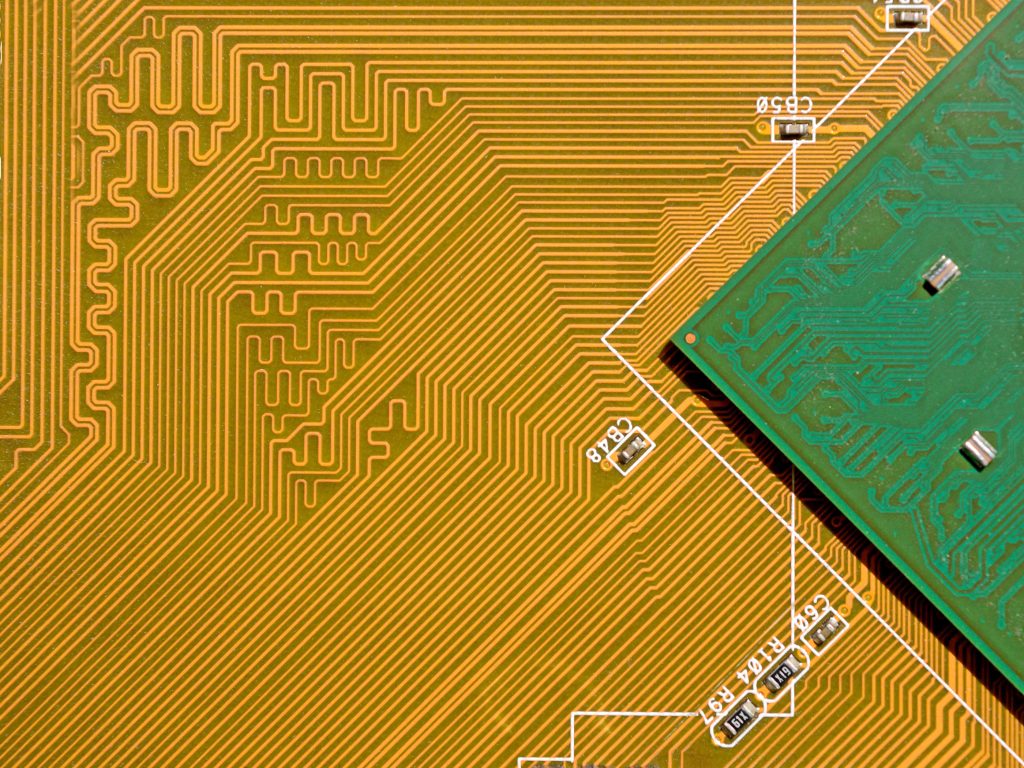
- Impedance Matching: Use controlled impedance traces (e.g., microstrip or stripline) and termination resistors to minimize reflections.
- Differential Pair Routing: Route high-speed signals (e.g., USB, HDMI) as differential pairs to reduce EMI and improve noise immunity.
- Length Matching: Ensure trace lengths are matched for critical signals (e.g., clock lines, data buses) to avoid timing skew.
EMI Mitigation Techniques
- Ground Plane Design: Implement a solid, low-impedance ground plane to minimize noise and provide a clear return path for signals.
- Shielding: Use shielded enclosures or guard traces to isolate sensitive circuits from noise sources.
- Decoupling Capacitors: Place decoupling capacitors close to IC power pins to suppress high-frequency noise and stabilize the PDN.
Power Delivery Network (PDN) Optimization
- Power Plane Stackup: Dedicate entire PCB layers to power and ground planes to reduce impedance and improve current distribution.
- Switching Regulators: Use switching DC-DC converters for high-efficiency in high-power conversion, complemented by LDOs for low-noise low-power applications.
- Thermal Management: Incorporate thermal vias, heatsinks, and copper pours to dissipate heat effectively.
Step-by-Step Technical Checklist for PCB Design
- Define Layer Stackup: Plan a multilayer stackup with dedicated power and ground planes.
- Control Impedance: Calculate and route traces with controlled impedance for high-speed signals.
- Minimize Crosstalk: Maintain adequate spacing between traces and use ground planes to isolate signals.
- Optimize PDN: Use bulk and decoupling capacitors to stabilize the power supply and reduce impedance.
- Thermal Analysis: Simulate thermal performance and incorporate heat dissipation techniques.
- Simulate and Validate: Use SI/PI (Signal Integrity/Power Integrity) simulation tools to verify design performance before fabrication.
Conclusion: Design for Performance and Reliability
A well-executed PCB design strategy ensures robust signal integrity, effective EMI control, and efficient power management. By addressing these technical challenges early, you can reduce debugging time, avoid costly redesigns, and accelerate your product’s time-to-market.
💡 Looking for Expert Guidance? MODMAG offers expert consultation to help you avoid pitfalls, cut costs, and speed up your product launch. Let’s connect and build a smarter hardware future! 🚀